We all make mistakes, and we are not ashamed to have to use printed circuit boards to correct them. Most of us are content to cut one or two tracks with xacto or add a jumper to make the circuit work. However, few of us will decide to actually operate inside the PCB itself.
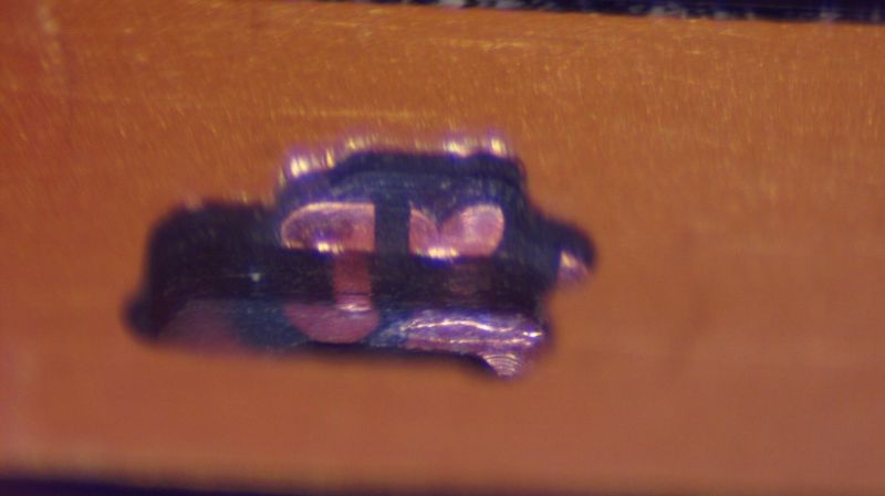
The story is, Andrew zonenberg was asked to debug some incredibly small PCBs for the prototype development board directly inserted into the USB Jack. The six-layer board was very dense and had a large number of blind holes. The twitter thread explained the debugging process in detail and finally found that one blind hole on the second layer was short circuited to the power rail and the other blind hole was short circuited to the ground. It also had [Andrew]’s fault Some beautiful lenses of the “mechanical tomography” method, which visualizes layers by slowly grinding the surface of the circuit board.
[Andrew] solved only one problem at the time of writing this article, but it must be believed. It starts by grinding off the PCB, using a ridiculously small end mill to contact the blind hole. The milled cavity [Andrew] ends up with only about 480 μ m × six hundred μ m. Only partially through the 0.8 mm thick plate, but this is enough to solve the problem of internal short circuit and add an internal bolt to fix the traces of damage during milling. The cavity is then filled with epoxy resin to stabilize the repair.
This debugging and repair technique is incredible. It reminds us of some internal chip welding repair, but it has completely entered another level. We can’t wait to see what the second repair looks like and whether the prototype of the development board can be salvaged.
Thank [esclear] for your reminder on this point.